| Nakamura Choukou Co., Ltd. (6166) |
|
||||||||


Company |
Nakamura Choukou Co., Ltd. |
||
Code No. |
6166 |
||
Exchange |
TSE Mothers |
||
Industry |
Machinery (Manufacturing) |
||
President |
Makoto Inoue |
||
Address |
27-27 Tsuruta-cho, Nishi-ku, Sakai-shi, Osaka prefecture |
||
Year-end |
End of March |
||
URL |
|||
* The share price is the closing price on December 12.
ROE and BPS are the value at the end of March 2016. |
||||||||||||||||||||||||
|
|
* The values for the term ending Mar. 2017 were estimated by the company.
Net income is profit attributable to the stock owners of the parent company. Hereinafter the same apply. This report introduces Nakamura Choukou Co., Ltd and the first half of fiscal year March 2017 earnings results and soon. |
|
| Key Points |
 |
| Company Overview |
|
Wafers (*)
A wafer is a flat functional part that is produced by thinly slicing ingots of electronic materials. It is made of various materials by purpose such as silicon, sapphire, SiC (silicon carbide) and GaN (gallium nitride). Silicon wafers are often used for IC chips and solar cells. Slicing business (*2) Business transferred to Nakacho Device Technology Corporation (an equity method affiliated company) in September 2013. Diamond nozzles (*)
A nozzle with sintered diamond at the tip, which is used for mounting electronic components on a print circuit board. By using diamond, the lifespan of the nozzle, holding capacity of the electronic component, image recognition efficiency and mounting efficiency are improved.  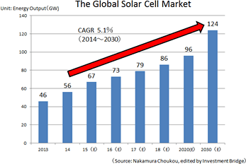  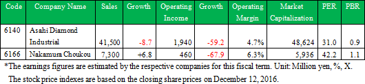 1. Segment
Nakamura Choukou's businesses consist of the three segments: Peripheral Business of Electronic Material Slicing, High-precision Equipment, and Chemical Fiber Spinning Nozzle Businesses.
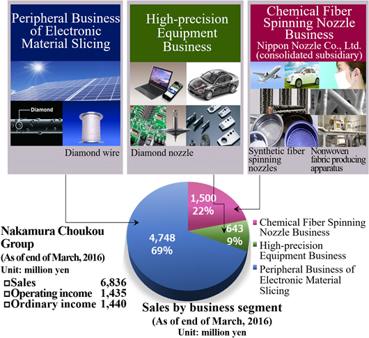 (1) Peripheral Business of Electronic Material Slicing
The development, manufacturing, and distribution of diamond wire which is used in the slicing silicon ingot during the manufacturing process of solar cells.
① What is Diamond wire?
Nakamura Choukou's diamond wire is used in the slicing process in manufacturing silicon wafers, which are used for the main part of a solar battery panel, that is, a solar cell.◎ Manufacturing Process of Silicon Wafer A "diamond wire" is a tool used to thinly slice rectangular silicon ingots that are pre-cut to the dimensions of each wafer. It is a threadlike slicing tool made with a thin piano wire with diamond granules firmly attached and is thinner than a human hair. The ingots are sliced by the diamond wires juxtaposed at short intervals and rotating at high speed over the guide rollers on a slicer. 2000 to 3000 silicon wafers are produced in 3 to 4 hours. The wafers are then cleaned and quality-inspected, treated to turn into cells, and incorporated into solar panel modules. 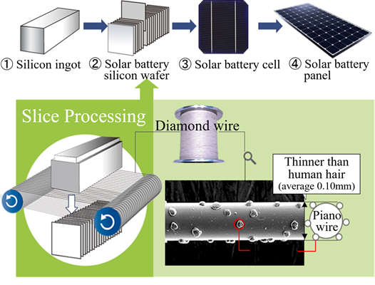 ②Diamond Wire Overview
There are two methods of slicing silicon wafers; "loose grain method" and "fixed grain method (using diamond wires)."
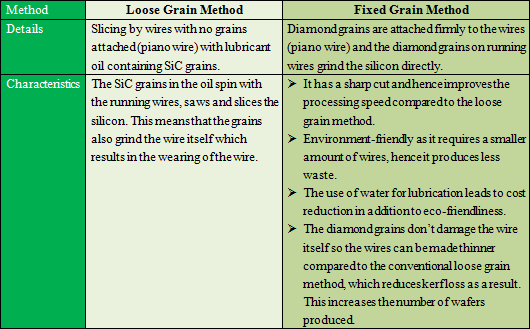 *kerf loss
Amount of the waste silicon when slicing. Kerf loss means material waste, so it must be kept minimum in order to reduce the manufacturing cost of solar battery panels. 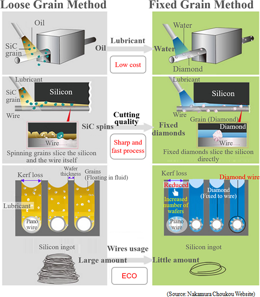 Nakamura Choukou had thinned the diamond wire to Φ(*)80 μm from the conventional standard of Φ100 μm and continues to create Φ70 μm and Φ60 μm diamond wires. (*) Φ
A symbol to indicate the diameter. Phi. (2) High-precision Equipment Business
Conduct the development, manufacturing and sale of high-precision equipment made of hard and brittle materials with high abrasion resistance such as diamond, cemented carbide and ceramic. The main products are diamond parts used in the engineering machines for manufacturing automobile parts and bearings and diamond nozzles, which are used in industrial machines for mounting electronic parts onto LCD television sets, smartphones, tablets, etc. In addition to high-precision parts and equipment, the company develops, manufactures and sells the cleaning machines for nozzles of the machines, etc. In recent years, the company has expanded its field to the development, manufacturing and sale of microreactor systems by combining micro high-precision technologies and device development technologies. The microreactor systems blend and synthesize fluid and gas in the micro environment by continuously and efficiently using chemical reactions. (For details, see 4. Growth strategy). The company also established Shanghai Nakamura Choukou Trading Co., Ltd. in February 2013. The purposes of this establishment are the expansion of the business in China and the improvement of customer support. These include expansion of trading with Japanese bearing manufacturers, cultivation of suppliers in China, expansion of the cleaning device business and establishment of the diamond wire user support system for the electronic material slicing business. (3) Chemical Fiber Spinning Nozzle Business
TThe designing, manufacturing and sale of chemical fiber spinning nozzles, the peripheral parts and nozzles and devices for nonwoven fabric.Nakamura Choukou started the domestic manufacturing of nozzles for chemical fibers (for production of rayon) and has been operating the business as a chemical fiber spinning nozzle manufacturer since its establishment in 1930. The spinning nozzle is a core manufacturing part which determines the quality of nonwoven and carbon fibers. The manufacturing of the nozzles requires delicate technologies in micro punching process and in the production of the devices, where Nakamura Choukou has provided for the market's needs with the technologies accumulated for many years in the same specialized industry. *The unique business model with the slicing business Suminoe Nakacho Device Technology provides Nakamura Choukou with the results of mass production tests as feedback. Nakamura Choukou then works on the improvement of the diamond wire based on the feedback. By combining the "technologies of diamond wire manufacturing" and "technologies of diamond wire usage" to create a synergy effect, the Company has made it possible to support its clients (silicon wafers manufacturers) in different technological perspectives and gain trust from them, which in turn has made its market expansion advantageous. This kind of business model is unique and makes Nakamura Choukou Group stand out. 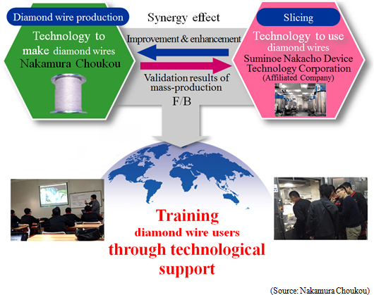 |
| First Half of Fiscal Year March 2017 Earnings Results |
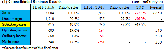 Downward Revision of Business Results, Having Operating Loss
The sales were 1,933 million yen, down 37.3% year on year. The sales of diamond wires, their main product, was affected heavily by the diminished trading volume arising from the sales price negotiation with their major clients, the worsening market climate surrounding silicon wafers for solar panels in China, the price drop due to intensified competition, and the stronger yen.Despite the effort to expand the sales volume to their new customers, the company failed to cover the decreased sales volume with their chief customers. The decreased sales resulted in a loss of all income items from operating income onwards. In August 2016, the 2Q and the full year forecasts were revised downwards. The actual results for the 2Q were even lower than the revised forecast. 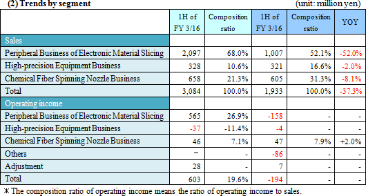 Decreased sales/operating loss As it bolstered the effort to diversify its clients, the number of clients has increased; however, it failed to cover the decreased trading volume with its chief client. <High-precision Equipment Business> Decreased sales/operating loss Shipping of nozzles for mounters and wear-resistant components for machine tools was steady. The cost reduction effort continued. <Chemical Fiber Spinning Nozzle Business> Decreased sales/increased profit The orders for nozzles came in more slowly than expected both inside and outside Japan, resulting in the decreased sales, but profit growth was recorded due to a reduction in fixed costs, etc. 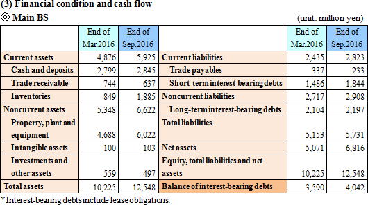 The total liabilities stood at 5,731 million yen, up 578 million yen, due to increased long/short term interest-bearing debts. Although retained earnings decreased, net assets grew by 1,744 million yen to 6,816 million yen because of the increased capital and capital surplus. As a result, equity ratio has risen by 4.7 points to 54.3% from the end of the previous term. 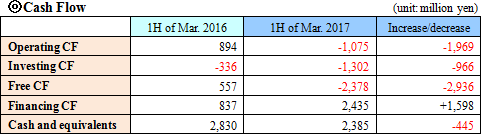 On the other hand, the acquisition of property, plant, and equipment increased outgoings, and investment CF grew further into the red, while free CF went into the red.Financial CF grew further into the black with the income generated by share issuance.Its cash position declined. |
| Fiscal Year March 2017 Earnings Estimates |
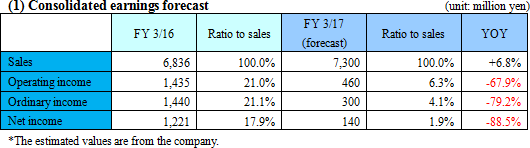 Full Year Results Forecast Unchanged, to See the Market Trend
The business performance for the 2Q was lower than the revised forecast released in August, but the full year forecast has not been revised. The company raised the following two points, considering that it is necessary to see their trends.
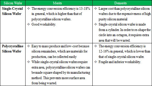 1) In the monocrystalline silicon wafer market, which is the biggest market for diamond wires with considerable competitions, the company searches for major clients who prioritize quality and has completed their assessments steadily. The company also leads the way in making diamond wires even thinner (Φ70μm, Φ60μm), winning the trust of the market for its products' functional stability. Based on this performance, the company is expected to enter into full-scale trading with multiple major clients including those outside China. 2) On the other hand, polycrystalline silicon wafers are brittle and harder to process, so although the size of its market is more than double that of the monocrystalline type, diamond wires are not widely used and therefore the competition is less severe.The company is developing higher quality wires and innovating technologies in the periphery of slicing operations to overcome the problems with the slicing of polycrystalline silicon wafers with diamond wires. Also in this department, based on these results, its products have been winning contracts from various major producers of polycrystalline silicon wafers and the sales are expected to commence. 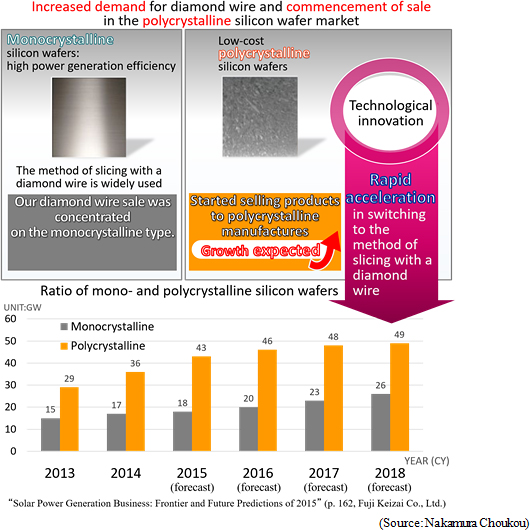 |
| About New Business |
|
① Microreactor Related Business
The conventional technology called "batch method", used in producing chemical goods produces the required chemical goods by combining a variety of raw materials and heating-cooling. However, although this method can synthesize large amounts at a time, there are many challenges including difficulty in mixing thoroughly. It is dangerous, large-scale equipment consumes enormous amounts of energy, and produces a large amount of waste products.On the other hand, flow synthesis technology enables the production of chemical goods by joining those flow paths, mixing, heating-cooling and isolation are done in the flows and optimal chemical reactions occur in machinery called microreactor in which a few tens to hundreds μm flow paths are provided. This brings great advantages such as energy-efficiency and improved safety and the social demand for this has been rapidly increasing. The company has been aiming to commercialize this microreactor system using their mold making technology with nanotechnology which they worked on in the process of research, development, and production of diamond nozzles and diamond wires. In particular, the company has started a joint development for autonomous automatic synthesis equipment, which leads to efficiency in the creation of pharmaceutical products, with the Biomedical Research Division of the National Institute of Advanced Industrial Science and Technology (AIST). Because the creation of pharmaceutical products requires a large amount of time and effort by human resources at the basic research stage to synthesize several hundred thousand compounds, this creates problems such as lowering the competitiveness of pharmaceutical manufacturers and increasing pharmaceutical prices. Given these circumstances, this project aims to provide solutions to these problems by developing an "autonomous synthesis equipment" which can automatically run 24 hours a day, 365 days a year to analyze, design and synthesize candidates for pharmaceutical products. The "autonomous synthesis equipment" the company is aiming to develop will create candidates for pharmaceutical products in 1/10 of the time of the conventional creation, and will contribute to shortening the time of new drug development and strengthening international competitiveness. With the opening of the "Flow Synthesis Laboratory" in September 2016, its development structure was strengthened. As the first step, it will undertake the synthesis and research of chemical products from pharmaceutical companies and public bodies, and launch its business undertaking such synthesis and research. As the second step, it aims to create a medicine venture using the accumulated knowledge of drug discovery. 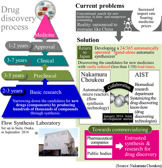 ②Zeolite Related Business
Zeolite is a substance that contains silica (silicon dioxide) and alumina (alminium oxide) as major ingredients, with characteristics of porous formation with many holes and has a large surface area, larger than a tennis court per 1 gram.These characteristics provide "adsorption", "ion exchange" and "catalytic" functions, and are used in various scenarios including the chemical field for treating catalysts to purify automobile emissions, the environmental field as an absorbent for radioactive cesium and the lifestyle field as an antibacterial agent for respirator masks. In general, there are already micron-size particles in the market but by making nanosized particles, basic performance will increase tremendously and expansion to new usages is anticipated However, conventional nano particle production methods were high in production cost, and detailed market evaluation has not been progressed. From this situation, the company has utilized the nanotechnology which they have been developing for a long time like microreactor related business together with the "pulverization-recrystallization" technique Tokyo University owns and started to develop the innovative process to make nanoparticle zeolite. As a result, they have succeeded in producing "nanosized zeolite" which has a diameter 1/100 of the size of ordinary zeolite at a low cost. (This "pulverization-reclystallization" process is patent pending) The company started pre-mass production in April 2016. After participating in exhibitions in Japan and China, the company has got a lot of inquiries. In August 2016, "Production method and particle-size control technology of zeolite nanoparticles" - a joint research between the company and the University of Tokyo - was selected for Stage III (NexTEP-A type) as part of Japan Science and Technology Agency's "A-STEP" (Adaptable and Seamless Technology Transfer Program through Target-driven R&D). A-STEP is a program to support technology transfer, specialized in the R&D phase aiming for practical application of the research findings in the field of science and technology, born out of academia and public research institutions that are significant in the national economy. The program covers various types of support categories according to respective R&D phases - the initial stage of research and development that acts as the phase to uncover candidate seeds from the research findings of the academia from the corporate points of view and to validate and actualize their potentials, the middle phase in which the tangible practicalities of the seeds are tested, and the final phase in which the business-led commercialization effort is effectuated to carry out the demonstration tests towards commercialization - and the program consists of three stages, namely Stage I, Stage II, and Stage III. Stage III (NexTEP-A type), for which the company was selected, is aimed at "commercializing the research outcomes of academia by supporting the large-scale, non-risk-free development by the businesses that utilize the seeds based on the researches in academia, and their practical application". The company expects that this decision will accelerate the process of their joint research. As R&D expenses are provided (fully redeemed by annual installments if development is successful; 10% redeemed otherwise), its effect in lowering the financial risk of having to fund the joint research cannot be overlooked. With aggressive PR activities, speedy market creation, and establishing low-cost/mid-volume production, it is planning to accelerate the pace of commercialization through industry-government-academia collaborations. 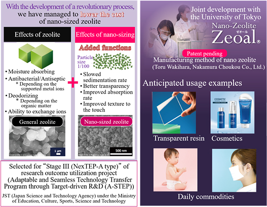 |
| Conclusions |
|
However, the company has not revised the full year forecast. It is of considerable interest to see if, as the company envisages, the market will continue to recover, and whether it will be able to satisfy investors' expectations and trust through the development of large-scale businesses in mono- and polycrystalline silicon wafers. Disclaimer
This report is intended solely for information purposes, and is not intended as a solicitation for investment. The information and opinions contained within this report are made by our company based on data made publicly available, and the information within this report comes from sources that we judge to be reliable. However we cannot wholly guarantee the accuracy or completeness of the data. This report is not a guarantee of the accuracy, completeness or validity of said information and opinions, nor do we bear any responsibility for the same. All rights pertaining to this report belong to Investment Bridge Co., Ltd., which may change the contents thereof at any time without prior notice. All investment decisions are the responsibility of the individual and should be made only after proper consideration.Copyright (C) 2017 Investment Bridge Co., Ltd. All Rights Reserved. |
